Understanding Common Troubleshooting Issues with XC7Z020-2CLG400I
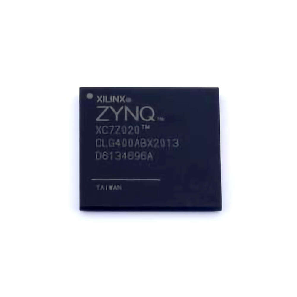
The XC7Z020-2CLG400I is a widely-used member of the Xilinx Zynq-7000 series FPGA s, combining Power ful processing capabilities with programmable logic in a single device. This integration makes it ideal for applications such as embedded systems, communications, automotive, and industrial control. However, like any complex piece of hardware, engineers may face challenges during the development and deployment of systems based on the XC7Z020-2CLG400I. In this article, we will discuss common issues that users might encounter and how to address them.
1. Power Supply Issues
One of the most common problems when working with FPGAs, including the XC7Z020-2CLG400I, is power supply instability. If the FPGA does not receive the correct voltage or if the power supply fluctuates, the device may fail to initialize or behave unpredictably.
Solution:
Ensure that the power supply meets the specifications outlined in the XC7Z020 datasheet. For the Zynq-7000 family, this typically involves providing 1.8V, 3.3V, and 1.0V for various internal components.
Use dedicated voltage regulators and ensure that the PCB design is optimized for stable power delivery. It’s also crucial to decouple the power rails appropriately with capacitor s placed near the FPGA's power pins to minimize noise.
Monitor the power rails during the initial power-up sequence to detect any issues.
2. Incorrect Pin Configuration
When designing with FPGAs, pin assignments are critical for ensuring that the signals from the FPGA map correctly to the external components (such as sensors, communication interface s, or Memory ). Incorrect pin configuration can lead to non-functional systems or miscommunication between the FPGA and peripherals.
Solution:
Double-check the pin assignments in the design constraints file (XDC) in the Vivado project. Ensure that each signal is routed to the correct I/O pin based on your design requirements.
Use Vivado’s “IO Planning” tool to visualize pin assignments and optimize them for routing and signal integrity.
Make sure to take note of the I/O standard required for each pin, as an incorrect I/O standard (e.g., LVTTL vs. LVCMOS) can result in logic errors or unreliable communication.
3. Configuration Failures
FPGA devices like the XC7Z020-2CLG400I require configuration data to program the internal logic. If there is an issue with the configuration process, the FPGA may fail to load the bitstream or behave unexpectedly after power-up.
Solution:
Verify that the configuration source (such as an SD card, JTAG, or SPI Flash) contains the correct bitstream and is properly connected to the FPGA.
Ensure that the configuration mode pins (such as MIO[15:0] for the Zynq-7000) are correctly set to the desired boot configuration mode.
If using external Flash memory for storing the bitstream, check the Flash programming and connection. Corrupted or improperly programmed Flash memory can cause configuration failures.
Test the configuration process through a JTAG connection for debugging. This can help determine whether the FPGA is not loading the bitstream properly.
4. Clock ing Issues
The XC7Z020-2CLG400I is a complex FPGA with multiple clock domains. Improper clocking setup can result in unstable or erratic behavior, as the FPGA may not correctly synchronize signals across different clock domains.
Solution:
Use Vivado’s clocking wizard to generate the correct clock constraints for your design. Ensure that you account for all clock sources, including external oscillators, internal PLLs , and any clock dividers or multipliers.
Review the Timing constraints and make sure that there is no clock domain crossing without proper synchronization.
If there are external clocks, use an oscilloscope to verify that the frequency and waveform meet the expected values.
Always ensure that the clock distribution network on the PCB is designed for signal integrity, with careful trace lengths and minimal noise interference.
5. I/O Interference and Signal Integrity Issues
As FPGAs deal with high-speed signals, improper routing or interference can affect the performance of I/O pins, leading to signal degradation or miscommunication.
Solution:
Use differential pair routing for high-speed I/O signals to improve signal integrity and reduce noise.
Keep trace lengths as short as possible and ensure that there is minimal via usage, as vias can introduce signal reflections and delay.
Use ground planes effectively to minimize electromagnetic interference ( EMI ) and ensure that I/O lines are shielded.
Test signals with an oscilloscope and use signal integrity analysis tools within Vivado to check for any issues in high-speed signal paths.
Advanced Troubleshooting Tips and Solutions for XC7Z020-2CLG400I
While basic issues like power supply instability and incorrect pin configurations are relatively easy to address, advanced users of the XC7Z020-2CLG400I may encounter more complex problems related to timing, memory interfaces, and debugging. Below, we explore solutions for some of these advanced troubleshooting scenarios.
1. Timing Violations and Setup/Hold Failures
Timing violations, particularly setup and hold time violations, are a common cause of FPGA malfunction. These occur when data does not meet the required timing constraints, which can result in incorrect operation or failure to meet the design’s functionality.
Solution:
Use Vivado’s Timing Analyzer to run a full static timing analysis. The tool will highlight any violations in setup and hold time.
Analyze the critical path for timing violations and consider optimizing it by adjusting the placement of critical components or adding additional logic to balance delays.
If necessary, use pipeline stages to break up long combinational paths and improve timing closure.
Ensure that the clock-to-output and setup-to-hold relationships are satisfied, and consider using clock domain crossing techniques, such as FIFOs or synchronizers, for data transfer between clock domains.
2. DDR Memory Interface Issues
The Zynq-7000 series, including the XC7Z020-2CLG400I, often interfaces with external DDR memory for high-bandwidth data storage. Problems in setting up DDR memory interfaces can result in system instability, crashes, or slow performance.
Solution:
Use Vivado’s Memory Interface Generator (MIG) IP to configure the DDR memory interface. The MIG IP is designed to handle the complex timing and signal integrity requirements of DDR memory.
Ensure that the DDR memory is properly initialized during power-up and that all necessary timing constraints are correctly applied.
Verify the PCB layout for the DDR memory traces, paying close attention to the impedance matching, trace length, and minimization of stub traces.
If the system shows instability, use a logic analyzer or oscilloscope to check the signals between the FPGA and DDR memory. Look for any clock misalignment or data corruption.
3. Debugging with Integrated Logic Analyzer (ILA)
When dealing with complex designs, sometimes the best approach to troubleshooting is to inspect the internal behavior of the FPGA in real-time. The Integrated Logic Analyzer (ILA) is a powerful debugging tool integrated into Vivado, allowing users to capture internal signals and troubleshoot without additional hardware.
Solution:
Add ILA cores into the design to monitor specific internal signals. This allows for dynamic tracing of signal activity, helping to pinpoint where the issue lies.
Use ILA in conjunction with the Vivado Debugger to set up breakpoints and step through the design.
The ILA can also be used to inspect timing violations or other internal issues, providing a non-invasive means of debugging without affecting the normal operation of the FPGA.
4. Thermal Management Issues
FPGAs such as the XC7Z020-2CLG400I can generate significant heat under high workloads, which can affect performance or even cause the device to overheat and fail.
Solution:
Ensure that the FPGA is properly cooled, particularly if it is running high-performance tasks or handling large amounts of data.
Use thermal management tools to monitor the temperature of the FPGA during operation. Many FPGA evaluation boards come with built-in temperature sensors.
Make sure the PCB design includes sufficient thermal vias, and use proper heat sinks or active cooling solutions if necessary.
5. Using the ZCU102 Development Board for Debugging
For those who are working with the XC7Z020-2CLG400I in a more advanced development environment, using a development board like the ZCU102 can be a helpful tool for debugging and troubleshooting.
Solution:
The ZCU102 development board includes a host of peripherals, memory, and debugging tools that can help you quickly validate your design in a controlled environment.
Use the onboard debugging tools such as JTAG, UART, and Ethernet for direct interaction with the FPGA, facilitating real-time debugging and analysis.
In conclusion, while working with the XC7Z020-2CLG400I FPGA, engineers may encounter several common and advanced issues. By following best practices in power management, signal integrity, clocking, and memory configuration, and by utilizing the built-in debugging tools in Vivado, these issues can be diagnosed and resolved quickly. The solutions provided here will help ensure that your Zynq-7000-based designs run smoothly, allowing you to take full advantage of the FPGA’s powerful features and capabilities.
If you are looking for more information on commonly used Electronic Components Models or about Electronic Components Product Catalog datasheets, compile all purchasing and CAD information into one place.

